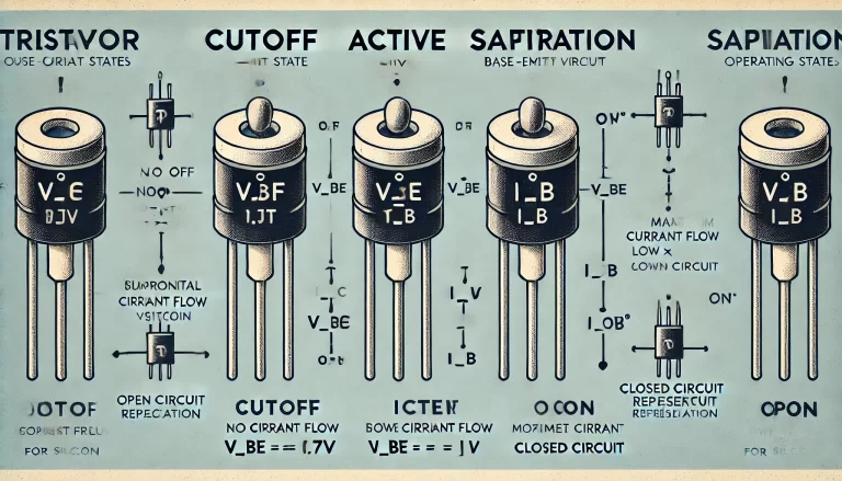
1. Cutoff State
Definition: In the cutoff state, the transistor is essentially “off,” meaning it does not conduct current from the collector to the emitter. This state occurs when there is insufficient base current, IBI_BIB, to activate the transistor, preventing it from allowing current flow between the collector and emitter terminals.
Conditions:
- **Base-Emitter Voltage V_{BE} < 0.7V** for silicon transistors** (or \( V_{BE} < 0.3V for germanium transistors): This low voltage across the base-emitter junction keeps it from turning on.
- Base Current IBI_BIB is zero or negligible: Without base current, the transistor cannot operate, meaning it effectively stops current from flowing through it.
Characteristics:
- The collector-emitter path behaves like an open circuit, meaning no current flows from the collector to the emitter.
- Collector current IC≈0I_C \approx 0IC≈0.
- Because there is no conduction between the collector and emitter, this state is often used to represent a switch in the “off” position in digital circuits.
Applications:
- Switching: In digital circuits, the cutoff state represents an “off” condition, where the transistor prevents current flow, similar to an open switch.
- Amplifiers: In some amplifier designs, the cutoff state can be part of an operating cycle where the transistor momentarily stops conducting.

2. Active or Linear State
Definition: The active state is the region where the transistor acts as an amplifier. In this state, the transistor allows controlled current flow from the collector to the emitter, proportional to the current applied to the base. This state is sometimes called the “linear region” because the output current is linearly related to the input current.
Conditions:
- **Base-Emitter Voltage V_{BE} \approx 0.7V** for silicon transistors** (or \( V_{BE} \approx 0.3V for germanium transistors): This voltage across the base-emitter junction is sufficient to forward bias it, allowing the transistor to conduct.
- Base-Collector Voltage ( V_{BC} < 0V or Collector-Emitter Voltage ( V_{CE} > V_{BE}: The collector-emitter junction remains reverse-biased, meaning the transistor stays in an amplifying state rather than fully turning on.
Characteristics:
- Current Amplification: In this region, the collector current ICI_CIC is proportional to the base current IBI_BIB, following the relationship IC=β×IBI_C = \beta \times I_BIC=β×IB, where β\betaβ (beta) is the current gain of the transistor.
- Linear Operation: The transistor operates in a region where the output is a predictable and controlled function of the input, which is why it is used in analog applications.
- Voltage Drop: There is a significant voltage drop across the collector and emitter (typically several volts), which indicates that the transistor is not fully “on” as it would be in saturation.
Applications:
- Amplifiers: This is the primary region used for amplifying signals in analog circuits, such as audio amplifiers or signal processing circuits.
- Analog Circuits: Transistors in the active region can be used in analog integrated circuits (ICs) where a steady and proportional relationship between input and output is needed.

3. Saturation State
Definition: In the saturation state, the transistor is fully “on,” meaning it allows maximum current flow from the collector to the emitter. This state occurs when both the base-emitter and base-collector junctions are forward-biased, causing the transistor to conduct as much current as the circuit allows.
Conditions:
- **Base-Emitter Voltage V_{BE} \approx 0.7V** for silicon transistors** (or \( V_{BE} \approx 0.3V for germanium transistors): This forward bias enables the base-emitter junction to conduct.
- **Collector-Emitter Voltage VCE≈0.2V V_{CE} \approx 0.2VVCE≈0.2V to 0.3V 0.3V0.3V: In saturation, the voltage drop across the collector-emitter junction is minimal because the transistor is allowing maximum current through, almost like a short circuit.
Characteristics:
- Maximum Collector Current: In saturation, the collector current ICI_CIC is limited only by the circuit (e.g., the external resistor and power supply), not by the transistor itself.
- Small Voltage Drop Across Collector and Emitter: A typical silicon transistor in saturation has a collector-emitter voltage VCEV_{CE}VCE around 0.2V to 0.3V.
- Switching Applications: In digital applications, saturation corresponds to the “on” or “closed switch” state, where the transistor allows current to flow freely, mimicking a closed switch.
Applications:
- Switching: In digital circuits, saturation is often used to represent an “on” state, such as in logic gates, microcontroller outputs, or other digital switching circuits.
- Power Electronics: Transistors in saturation can be used in applications like motor drivers or power control circuits where a fully “on” state is needed to supply current to a load.
Summary of Transistor States
| State | VBEV_{BE}VBE (Silicon) | VCEV_{CE}VCE | ICI_CIC | Application |
|---|---|---|---|---|
| Cutoff | <0.7V< 0.7V<0.7V | Large (open circuit) | ≈0\approx 0≈0 | Digital “off” |
| Active | ≈0.7V\approx 0.7V≈0.7V | >VBE> V_{BE}>VBE | IC=β×IBI_C = \beta \times I_BIC=β×IB | Amplification |
| Saturation | ≈0.7V\approx 0.7V≈0.7V | Small (close to 0V) | Maximum (limited by circuit) | Digital “on” |
Understanding these states and the conditions that define them allows designers to use transistors effectively in a variety of circuits, from amplifiers to digital switches. Each state leverages the unique characteristics of the transistor to perform specific functions in electronic devices.
